Semiconductor Manufacturing and Cleanroom Requirements
Introduction
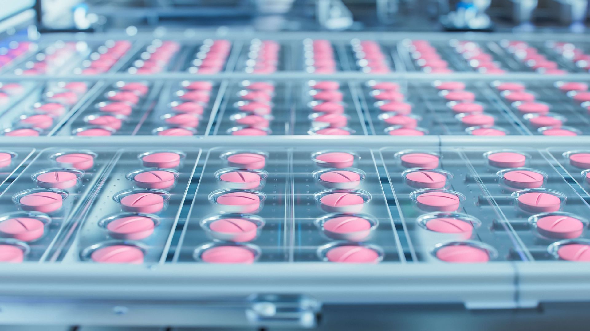
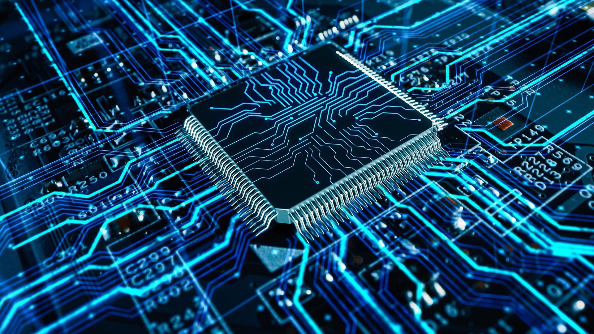
Semiconductor manufacturing is a cornerstone of modern technology, enabling the production of integrated circuits (ICs) that power everything from smartphones and computers to automobiles and medical devices. This highly intricate process involves multiple steps of precision engineering and fabrication. The production environment, especially the cleanroom, plays a critical role in ensuring product quality and yield.
Cleanrooms are meticulously controlled environments designed to minimize contamination from particles, microbes, and chemical vapors, as even microscopic contaminants can ruin semiconductors. This article delves into the intricacies of semiconductor manufacturing, the stringent requirements of cleanrooms, and the interdependencies between the two.
Semiconductor Manufacturing Process
The manufacturing of semiconductors is a multi-step process that transforms silicon wafers into functional chips. Each stage requires advanced equipment, materials, and environmental controls to achieve the high levels of precision needed for modern semiconductors.
1. Silicon Wafer Preparation
- Raw Material Extraction: The process begins with high-purity silicon, derived from quartz or sand, which undergoes chemical purification.
- Crystal Growth: Using the Czochralski process, a single crystal ingot is grown by pulling a seed crystal from molten silicon.
- Wafer Slicing and Polishing: The ingot is sliced into thin wafers, polished to a mirror finish, and cleaned to remove impurities.
2. Photolithography
This is a core step in patterning the microscopic circuits on the wafer.
- Coating with Photoresist: A light-sensitive material is applied to the wafer surface.
- Mask Alignment and Exposure: A photomask defines the desired pattern, which is transferred onto the photoresist through exposure to ultraviolet (UV) light.
- Development and Etching: The exposed photoresist is developed, leaving a precise pattern that allows for selective etching of the wafer.
3. Etching and Deposition
- Etching: The unwanted material is removed either through wet chemical etching or dry plasma etching.
- Deposition: Layers of materials like silicon dioxide or metal are deposited using techniques such as chemical vapor deposition (CVD) or atomic layer deposition (ALD).
4. Doping
Doping introduces impurities into specific areas of the silicon wafer to modify its electrical properties. This is typically done using ion implantation, where ions are accelerated into the wafer under precise conditions.
5. Metallization
This step involves depositing and patterning metal layers that form the electrical connections between transistors.
6. Testing and Packaging
Before chips are packaged, they are subjected to rigorous testing to ensure functionality. The wafers are then diced into individual chips, packaged, and further tested.
Cleanroom Requirements in Semiconductor Manufacturing
Cleanrooms are essential for maintaining the quality and reliability of semiconductor products. Contamination during any stage of the manufacturing process can lead to defects, reducing yield and increasing costs.
1. Key Contamination Risks
- Particulate Matter: Dust, fibers, and other particles can interfere with photolithography or cause short circuits.
- Chemical Contamination: Vapors from outgassing materials can react with sensitive processes or materials.
- Microbial Contamination: Bacteria and other microorganisms can introduce particulates or biological residues.
- Electrostatic Discharge (ESD): Static electricity can damage the microscopic features on a chip.
2. Cleanroom Classifications
Cleanrooms are classified based on the maximum allowable particle count per cubic meter of air. The most common standards are:
- ISO 14644-1: Defines classes from ISO Class 1 (cleanest) to ISO Class 9 (least clean).
- Federal Standard 209E (Retired but still used): Defines classes as Class 1, 10, 100, etc., representing particle counts per cubic foot of air.
For semiconductor fabrication:
- Photolithography and deposition areas often require ISO Class 3 or Class 4.
- General manufacturing areas may use ISO Class 5 or higher.
3. Environmental Controls
- Temperature and Humidity: Temperature is maintained between 20-22°C (68-72°F) with variations under ±1°C. Humidity is controlled to prevent condensation or electrostatic issues, typically at 30-50%.
- Airflow and Filtration: High-efficiency particulate air (HEPA) filters or ultra-low penetration air (ULPA) filters ensure clean air. Laminar airflow minimizes turbulence and particle deposition.
- Pressure: Cleanrooms are kept at positive pressure relative to surrounding areas to prevent ingress of contaminants.
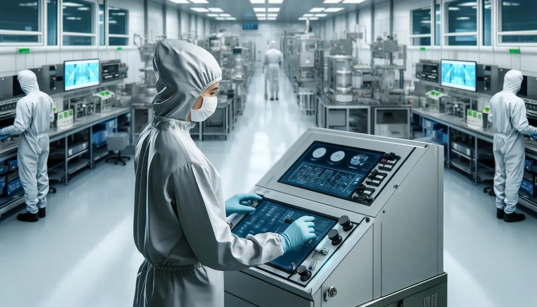
4. Personnel and Equipment
- Garments: Operators wear cleanroom suits (bunny suits) made of non-linting materials. Gloves, masks, goggles, and shoe covers prevent particle shedding.
- Behavior Protocols: Movement is minimized to reduce particle generation. Strict no-touch policies are enforced for sensitive surfaces.
- Equipment Cleanliness: Tools are cleaned regularly, and materials are stored in particle-free environments.
5. Monitoring and Maintenance
Continuous monitoring ensures that cleanroom parameters stay within specification.
- Particle Counters: Measure air quality in real time.
- Environmental Sensors: Monitor temperature, humidity, and pressure.
- Preventative Maintenance: Regular servicing of filters, equipment, and systems prevents contamination risks.
Advances in Cleanroom Technology
As semiconductor processes evolve, cleanroom technology must adapt to meet stricter requirements.
- Nanotechnology Applications: Cleanrooms for <3 nm semiconductor processes demand sub-ISO Class 1 environments.
- AI and IoT Integration: Smart sensors and AI-driven systems provide predictive maintenance and real-time optimization.
- Sustainability Initiatives: Efforts to reduce energy and water use include efficient HVAC systems and closed-loop water recycling.
Conclusion
Semiconductor manufacturing relies heavily on advanced cleanroom environments to ensure the integrity of the fabrication process. As chips become smaller and more complex, the demands on cleanroom technology will continue to increase, driving innovations in contamination control, environmental sustainability, and real-time monitoring. Ensuring adherence to these stringent cleanroom requirements is critical for producing reliable, high-performance semiconductor devices.
Read more: All About Cleanrooms - The ultimate Guide